
High-Throughput Fabrication of Large-Scale Metaholograms via One-step Printing
Metasurfaces,
which are designed by arranging meta-atoms, have attracted attention for their
ability to create optical properties that do not exist in nature. However,
previous methods for fabricating metasurfaces
using electron-beam lithography (EBL) are expensive and have limited production
capacity, inhibiting mass production. In this study, a new manufacturing method
is demonstrated using an argon fluoride (ArF)
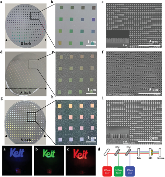
scanner and nanoimprint lithography (NIL) to overcome these limitations. 266
millimeter-scale metasurfaces
are designed and fabricated on an 8-inch wafer using an ArF
scanner. Subsequently, this is used as a master stamp to replicate the metasurfaces
in an 8-inch wafer scale through the NIL process all at once. To demonstrate
the effectiveness of this method, a metahologram
is designed and manufactured using TiO2 nanoparticle-embedded-resin (nano-PER).
The metahologram
achieves an 81.2% yield during replication, with a maximum efficiency of 60.7%
at 450 nm, 45.1% at 532 nm, and 38.5% at 635 nm, respectively. The results
demonstrate the production of practical metaholograms
using low-cost and high-throughput processes.